Create Symbols
Symbols are useful when the schematic design
is done hierarchically. At a higher of level of abstraction, we would like
to use a symbol to replace the details of a cell. Because of this, a symbol
of a cell design should define all the inputs and outputs of that cell.
There are two ways to create a symbol. If you
have a schematic design already, you can create its symbol right from the
cell. If you don't have a schematic design yet and you want to create a
symbol for the cell, you can start from scratch.
- Create a symbol from an existing schematic
- Create a symbol from scratch
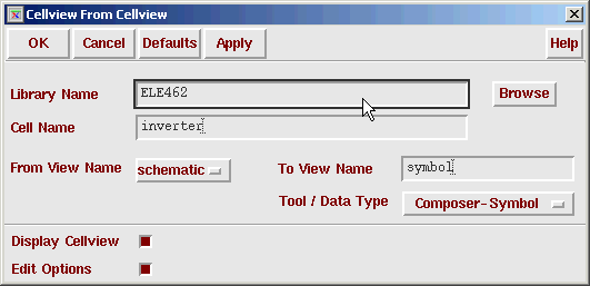
Click on Design->Create Cellview->From Cellview menu in the symbol edit window, a pop up dialogue box will appear. We can use the default setup in this window to create the symbol.

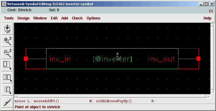
This will pop-up another window that contains a default symbol picture. It has a red box that encloses the green colored inverter symbol. This red box defines the actual size a symbol will occupy, if you were to use this inverter in another design. You can change the size of this box. It is good custom to exactly fit the symbol within the red box. The red square dots indicate the pin connections. [@InstanceName] and [@PartName] are display variables, which you may delete or keep. The following picture shows the symbol.

If you don't like this rectangular symbol that
is automatically created by the tool, you can create a symbol of you own.
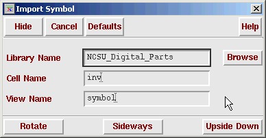
As long as we know the inputs and outputs of a cell, we can create a symbol for it. We can either draw the lines and arcs ourselves (which is pretty self-explanary and the hot keys are very much similar to the schematic composer window), or we can borrow some existing drawings and modify them. Click on Add->Import Symbol... and the following dialogue box appears.

Click on Browse to find a symbol in other libraries. In our case, we borrowed the symbol from cell inv of library NCSU_Digital_Parts. Since these two designs are essentially the same, they have exactly the same number of input/output pins. We only have to modify the input and output pin names so that they conform to the pin names in our schematic design. The final symbol is shown below.
